
What “SMT PNP Process” Means
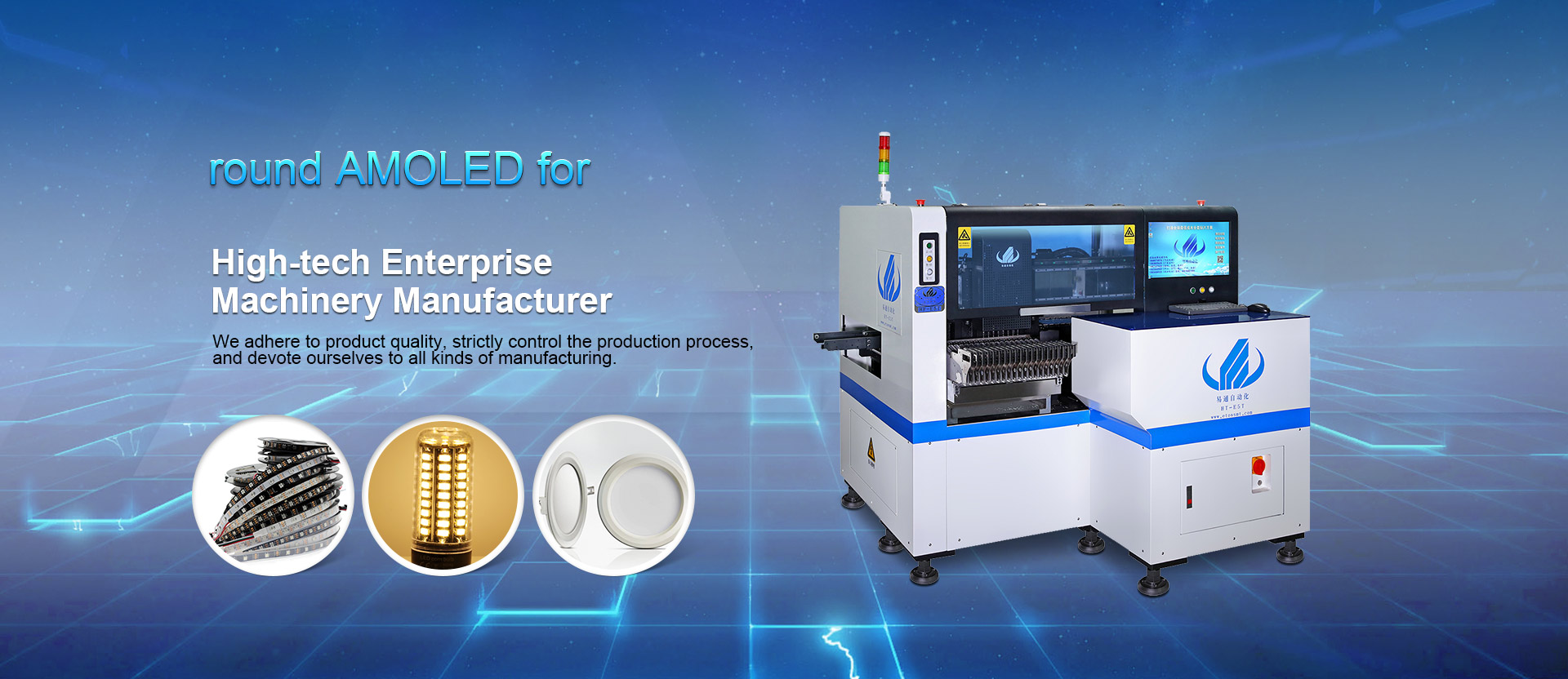
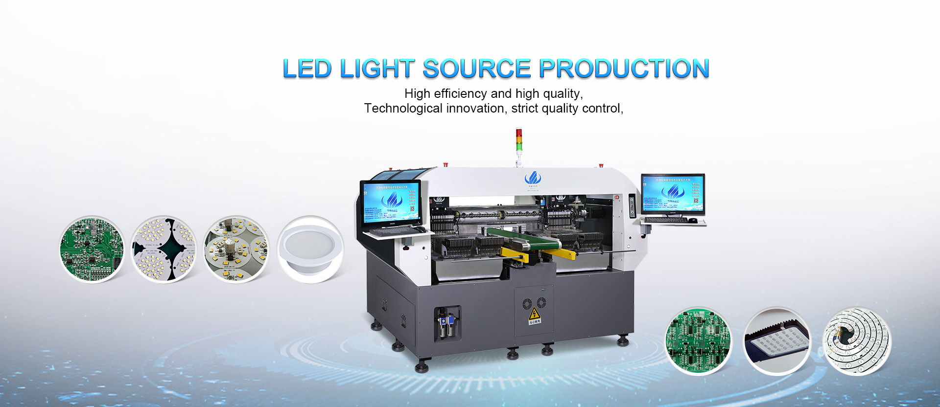
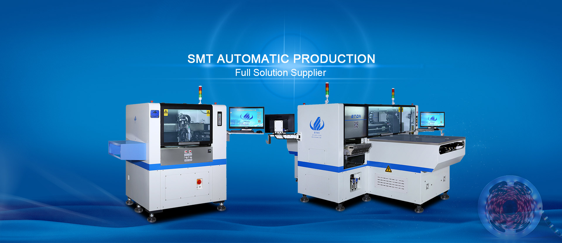
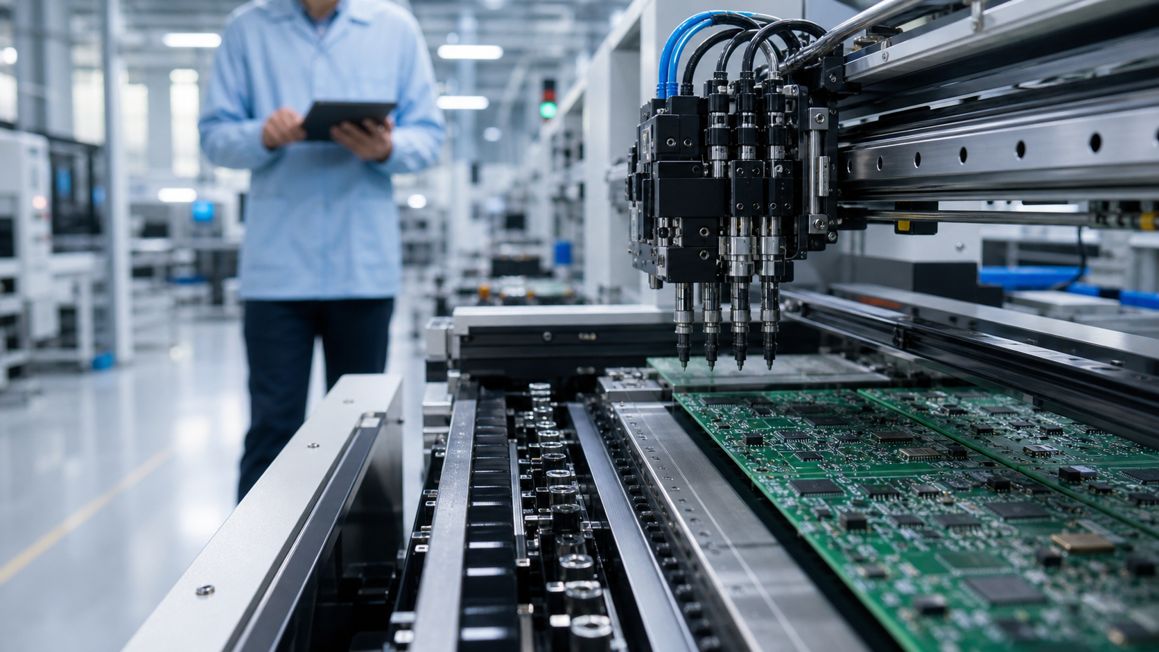
The SMT PNP process is the pick-and-place stage of surface-mount manufacturing. It is where a programmed placement system collects components from feeders, verifies them with vision, and positions them accurately on solder-pasted PCBs. Because this stage connects incoming component preparation with reflow and inspection, it has a major effect on both throughput and defect prevention.
Step 1: Prepare Boards, Feeders, and Programs
Before production starts, operators verify the board revision, solder paste condition, stencil setup, component reels, feeder locations, and placement program. Barcode control and feeder verification reduce the risk of loading the wrong component. The program should include component libraries, rotation, polarity, fiducial strategy, nozzle selection, and board support settings. This preparation is often the difference between a smooth launch and avoidable downtime.
Step 2: Align and Place Components
The machine transfers each board into position, finds global and local fiducials, picks components, and uses its vision system to confirm orientation and placement. It then places parts according to the programmed coordinates. Fine-pitch devices, small passives, connectors, and LEDs can require different nozzles, pickup heights, and placement parameters. A robust SMT PNP process applies the correct rules to each package family instead of treating every component alike.
Step 3: Reflow and Inspect the Assembly
After placement, the PCB enters the reflow soldering process. The temperature profile must match the solder alloy, board mass, and component limits. Automated optical inspection then checks for issues such as missing parts, polarity, offset, tombstoning, and selected solder defects. If a defect pattern appears, the team should trace it back to printing, feeder setup, placement parameters, or reflow rather than relying only on rework.
Measure the Metrics That Improve the Line
Track first-pass yield, placement defects per model, feeder-related stoppages, changeover time, utilization, and rework causes. These metrics reveal whether the constraint lies in programming, materials, equipment, or operator workflow. They also make it possible to compare a proposed pick and place solution against real production needs rather than nominal capacity.
Turn the Process into a Scalable Solution
For a new line or an upgrade, map the whole PCB board assembly process: printing, placement, reflow, inspection, handling, and data collection. Submit product files and a target output to receive a balanced line recommendation. A solution designed around actual components and quality requirements is easier to run today and easier to expand for the next production season.
Post time: Jul-30-2026